One of the most fascinating aspects of hardware hacking is transforming a device to perform tasks far beyond its original design. This process is inherently creative, often disruptive, and undeniably enjoyable. Every hacker approaches these challenges uniquely, influenced by their methodologies, habits, and skill sets. This article details one such approach, focusing on the journey rather than just the outcome, using an OBD2 reader as the subject of modification.
Introduction
This project, initially developed for 44CON, explores the potential of modifying an off-the-shelf OBD2 reader. The goal was to repurpose this diagnostic tool into a versatile USB emulation and exploitation device. Several key features were desired for the target device:
- LCD screen for user interface and feedback
- Menu buttons for navigation and control
- USB device communication for data transfer and interaction
- Onboard storage for storing payloads and data
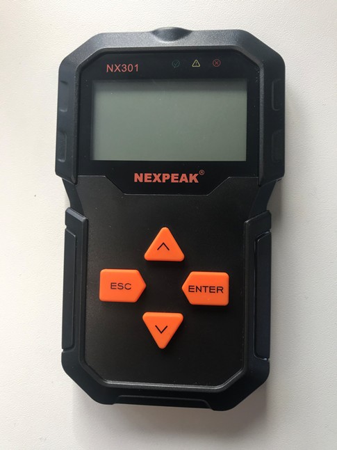
OBD-II readers, commonly used for vehicle diagnostics, emerged as ideal candidates due to their potential hardware capabilities. A colleague’s prior reverse-engineering work on OBD2 readers further solidified this direction. After a thorough search for a suitable device, the Nexpeak NX301 was identified as possessing the necessary features for this ambitious project.
A preliminary examination of the Nexpeak NX301’s internal components confirmed its suitability. Key hardware specifications that made it perfect for this project included:
- STM32F103 MCU: Featuring 64KB of Flash and 20KB of RAM
- 72MHz Maximum Clock Speed: Providing ample processing power
- Integrated Peripherals: Including an LCD screen, USB Interface, CAN interface, and menu buttons
- 8MB SPI Flash Memory: Offering substantial onboard storage
This particular OBD2 reader, and similar models available under various brands, appeared to share the same core functionalities, making it a consistent and accessible platform for experimentation.
Firmware Analysis
Initial investigation revealed that the USB interface of the OBD2 reader was primarily intended for firmware updates. A dedicated firmware update tool was available for download online, suggesting a straightforward update mechanism.
Examining the program files of the firmware update tool indicated the use of a standard STM32 USB CDC interface for firmware uploading. This implied the utilization of standard system libraries, simplifying the potential for custom firmware development. Network analysis using Wireshark revealed that the firmware files were downloaded via HTTP, making it easy to locate and download the firmware directly for analysis.
However, a quick analysis of the downloaded firmware payload revealed that it was heavily encrypted. This meant a direct, easy modification of the existing firmware was not immediately possible.
Further complicating matters, connecting directly to the STM32 microcontroller on the OBD2 reader board showed that it was read-out protected. While the firmware could not be read directly from the device, it was still possible to overwrite it. At this stage, two primary paths emerged:
Option 1: Building Firmware from Scratch
- Advantage: Bypasses the need for software reverse engineering of the original firmware.
- Advantage: Allows full control over the 64KB of flash memory.
- Disadvantage: Requires hardware reverse engineering to understand peripheral connections.
- Disadvantage: Disables the use of the device’s built-in firmware update functionality.
Option 2: Breaking Readout/Firmware Protection
- Advantage: Enables modification of the original application, potentially leveraging existing functionalities.
- Advantage: Could allow for the continued use of the built-in firmware update mechanism.
- Disadvantage: Requires identifying and exploiting a weakness in the device’s security.
- Disadvantage: May not grant full access or control compared to custom firmware.
Ultimately, a dual approach was adopted, pursuing both building custom firmware and attempting to break the existing firmware protections.
Building Firmware From Scratch
The first step in creating custom firmware involved establishing a direct programming interface. Soldering an SWD (Serial Wire Debug) header to the conveniently located pads on the OBD2 reader’s circuit board enabled easy firmware flashing, even with the device case closed.
While logic analysis of the original peripherals before code deletion is generally recommended, in this instance, the decision was made to assess peripheral functionality from datasheets. This approach proved straightforward for the SPI Flash and CAN interfaces due to readily available documentation. However, the LCD screen presented a greater challenge.
A crucial aspect of hardware assessment is tracing the connections of standard peripherals to the microcontroller pins. This was relatively simple for components directly connected to pins, such as menu buttons and LEDs. With the hardware layout understood, a new project was initiated using STM32Cube design software. Each pin was labeled, and the SPI, USB, and CAN interfaces were configured accordingly within the development environment.
The SPI Flash memory was mapped to the SPI2 port, allowing for the use of standard SPI flash commands for data communication. Furthermore, STM32Cube’s built-in USB libraries offered the flexibility to emulate virtually any USB device class, providing the capability to spoof various hardware functionalities.
Reverse Engineering the Screen
The LCD screen, identified by the part number DJM12864G13, unfortunately lacked publicly accessible datasheets. However, online sales pages provided pinout diagrams, which greatly aided in understanding the function of each pin.
Tracing each pin and analyzing the pinout revealed that the LCD operated in parallel mode. By sending test packets based on command/data and read/write signal information gleaned from the pinout, the underlying communication protocol began to emerge. It was determined that the LCD used a standard protocol common to LCD controllers from various manufacturers who did provide datasheets. Leveraging these alternative datasheets allowed for establishing proper communication with the OBD2 reader’s LCD controller.
This reverse engineering effort culminated in the ability to display ASCII bitmaps on the LCD screen, marking a significant step in controlling the device’s user interface.
Further investigation into the protocol revealed the capability to display images, albeit with some added complexity in implementation.
USB Connectivity for Expanded Functionality
With the display functional, attention shifted to the USB interface. The goal was to create a device that could act as both a USB disk for file storage and retrieval, and a USB keyboard for automated command input. The LCD screen and menu buttons would facilitate file selection for keyboard emulation.
Fortunately, STM32Cube provided ready-made libraries for standard USB device classes, including HID (Human Interface Device) and Mass Storage. These libraries were instrumental in emulating a USB drive and keyboard. The Mass Storage library was paired with the onboard SPI flash memory, effectively creating 8MB of storage accessible via USB.
The custom firmware was designed to operate in two distinct modes. Upon startup, if a menu button was held, the device would enumerate as a USB disk. The SPI Flash was formatted with a FAT32 filesystem, enabling standard file operations.
Read and Write commands from the USB Mass Storage libraries were translated into corresponding SPI Flash read and write commands. A key difference was the block size; USB disk operations typically use 4096-byte blocks, while the flash memory operated on 256-byte blocks. This required translating each USB block read/write into 16 flash memory operations.
If no buttons were held during startup, the OBD2 reader would present itself as a USB keyboard to the host computer. To enable menu-driven file selection for keyboard emulation, the FATFS library was integrated. This library allowed for mounting, reading, and writing FAT32 filesystems, with customizable callback functions for hardware integration. This enabled reading files from the SPI flash and displaying their contents on the LCD screen.
To translate text file content into USB keyboard input, a mapping from ASCII characters to USB HID scancodes was necessary. This was achieved by creating a simple lookup table that converted characters into their corresponding scancodes.
Due to hardware limitations, a few development shortcuts were implemented. The USB interface would only enumerate upon initial connection to a host computer. Therefore, mode selection (Mass Storage or Keyboard) was determined at startup by holding down specific buttons. Changing modes required physically disconnecting and reconnecting the OBD2 reader from the PC.
This culminated in a functional device that met the initial project goals. However, deploying this custom firmware to a completely new, unmodified Nexpeak OBD2 reader was not yet possible without hardware modification, as the original firmware protections remained unbroken.
Cracking Firmware Encryption for Unrestricted Access
To reiterate, the security measures in place were:
- Encrypted Firmware Update Payload
- Code Readout Protection Enabled
- No Readily Available Generic Exploits for the STM32F103
While the STM32F103 is known to be susceptible to glitching attacks, this would involve physical modification of the board. Other, less invasive options were explored first.
A significant vulnerability lay in the fact that SWD debugging was enabled in Firmware Upgrade mode. Despite readout protection preventing flash memory access, RAM could still be read at any time. This proved crucial for extracting key information potentially stored in RAM during the firmware update process.
Furthermore, the use of standard USB CDC communication for firmware updates made it feasible to intercept and analyze these updates using a man-in-the-middle (MITM) attack.
Using a BeagleBone Black and the USBProxy USB analysis tool, the firmware update process was monitored. This approach is also achievable with other embedded Linux devices possessing USB device capabilities, such as Raspberry Pi Zero or NanoPi.
Analysis of the captured USB communication revealed that the update process could be replayed using LibUSB. However, CRC (Cyclic Redundancy Check) values appended to commands would need to be recalculated if the payload was modified.
A tool was developed to emulate and replay the firmware update sequence. Each packet could be individually replayed and validated based on the device’s responses. The CRC algorithm in use was identified as the standard X.25 CRC-16, which is easily calculable, allowing for payload modifications. The update process transferred data in 512-byte blocks.
Initial examination of the firmware update file indicated a size consistent with the chip’s memory capacity, suggesting the absence of conventional integrity checks. This was confirmed by the device failing to boot when a corrupted firmware payload was uploaded. The ability to upload older firmware versions further demonstrated the lack of rollback protection.
By interrupting the firmware update process after each 512-byte block, it became possible to pinpoint the memory location in RAM where the firmware payload was decrypted and stored. The first two 32-bit blocks of Cortex-M chips (like the STM32F103) always end with 0x20 and 0x08 respectively, providing a recognizable signature in memory.
This allowed for manual extraction of the decrypted firmware from RAM and subsequent reconstruction of the complete firmware image. While decryption was achieved, writing new firmware required understanding the encryption algorithm and keys, which remained unknown. The device also exhibited crashes after each RAM read, hindering further dynamic analysis.
Although the encryption algorithm wasn’t immediately apparent from the RAM dump, it was highly probable that encryption keys were also stored in RAM. If the encryption algorithm could be identified, these keys could then be used to both decrypt and encrypt firmware.
To deduce the encryption algorithm, a strategy of educated guessing and observation was employed. Subtle modifications were made to the first 512-byte block of the encrypted firmware to observe their impact on the decrypted firmware in RAM. This iterative process aimed to narrow down the likely encryption algorithm.
Starting with a simple approach, a single byte in the encrypted firmware was altered. If only a single byte changed in the decrypted firmware, it would suggest a stream cipher.
If modifying a byte resulted in changes only within the first few bytes of the decrypted firmware, it would point towards an ECB (Electronic Codebook) mode block cipher, likely AES (Advanced Encryption Standard).
If modifying a byte in a later part of the firmware caused changes in all subsequent blocks of decrypted data, it would indicate a CBC (Cipher Block Chaining) mode block cipher.
However, in this case, modifying any byte in the encrypted payload resulted in a complete change in the entire decrypted firmware image. This strongly suggested that the encryption algorithm was likely Block TEA (Tiny Encryption Algorithm) or XXTEA (Corrected Block TEA).
Based on this hypothesis, the first 512-byte block of encrypted firmware and the RAM dump were processed together, iterating through blocks within the RAM dump.
This analysis revealed the beginning of the decrypted firmware within data located near the start of the RAM dump. This successful correlation indicated that the XXTEA key had been found.
The recovered XXTEA encryption keys were:
- key[0] = 0x00001494;
- key[1] = 0x0000d65b;
- key[2] = 0x05e2e03f;
- key[3] = 0x00005426;
Dumping the Bootloader for Complete Device Control
With the encryption keys in hand, deploying custom firmware to the OBD2 reader became possible. However, the next objective was to extract the bootloader responsible for secure firmware updates.
By modifying the original firmware payload, now decryptable and encryptable with the recovered keys, the firmware could be overridden to dump the entire contents of the bootloader into RAM.
This dumped bootloader could then be read from RAM and preserved, allowing for restoration of the device if the flash memory was ever accidentally erased. A small ARM payload was crafted to ensure this persistence.
This payload, when executed, first wrote a magic number (0xBBAA) to the beginning of RAM, followed by a loop that read the entire flash memory content and wrote it to the remaining RAM space. Finally, it entered an infinite loop to halt further processing. This code was quickly assembled using an online assembler like the one provided by shell-storm.org. The compiled code needed to be inserted into the update payload.
To determine the correct insertion offset within the firmware, the reset vector address (0x04 in the binary) of the microcontroller was examined. The reset vector was found to be 0x08004101. By subtracting the flash start address (0x08000000) and the bootloader size (0x4000), and removing the Thumb code indicator bit (lowest bit set), the offset 0x100 was calculated as the correct location to inject the assembled payload.
After running this modified firmware, dumping the RAM revealed the magic number (0xBBAA) followed by the complete bootloader image.
This successful bootloader extraction provided complete insight into the device’s original firmware update process and internal workings.
Gaining knowledge of the firmware update procedures enabled firmware deployment without requiring hardware modifications. Sensitive information within the firmware could be extracted. Modification of the existing firmware became feasible, and access to the bootloader ensured device recoverability in case of accidental flash erasure. Collectively, this level of access allowed for repurposing the OBD2 reader for virtually any desired function without physical hardware changes. However, to further explore the device’s potential, hardware modifications were also undertaken.
Modifying the Hardware for Expanded Capabilities
Simple hardware modifications can add significant features to embedded devices. Removing unnecessary components can free up resources for new functionalities.
The CAN interface, while central to the OBD2 reader’s original purpose, was not needed for the intended new applications.
Therefore, the CAN interface components were removed from the design, and the associated microcontroller pins were re-allocated as timer and interrupt pins.
These re-purposed pins were sufficient to replicate previous work on creating NFC tag emulation devices.
The components for the CAN communication were desoldered from the OBD2 reader PCB, and wires were soldered in their place to connect a custom NFC daughterboard.
Using a previously developed standard design, a small daughterboard for NFC emulation was fabricated and connected to these wires.
An antenna was then attached to the daughterboard and routed to the back of the device case.
Leveraging the software developed for the USB emulation device, the USB Mass Storage functionality was used to store binary NFC tag data on the OBD2 reader. This data could then be selected and used for NFC tag emulation.
The 72MHz clock speed of the STM32F103 microcontroller ensured that the existing software could be ported almost directly to the new hardware configuration. The LCD screen served as the interface for selecting NFC tag data loaded via USB.
A readily available Lithium-Ion battery was taped to the back of the device and connected directly to the SWD pins to provide power.
With minor adjustments to the FATFS library to accommodate memory constraints, the project culminated in a fully functional 13.56MHz NFC tag emulator with a menu-driven interface, all built around a repurposed OBD2 reader.
Video Demonstration
[Link to Video Demonstration – Placeholder, Insert Actual Link Here]
Conclusion
Modifying both the software and hardware of embedded devices like an OBD2 reader is a challenging yet deeply rewarding endeavor. It cultivates valuable skills in development and reverse engineering that are broadly applicable within IoT security. Furthermore, it offers a path to breathe new life into discarded electronics, transforming them into something far more interesting and useful.
Taking apart and experimenting with your old devices before discarding them is highly recommended. You might be surprised at the creative repurposing possibilities that await.